 |
|
|||||
 |
|
www.pcbco.com.au N0. 18 Tuas South Street 3 Jurong Industrial Estate, Singapore Phone: +65 6862-0802 Fax +65 6862-0800 Email: info@pcbco.com.au |
||||
|
|
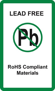
Introduction The European Union has implemented two directives targeting environmental impact. These directives are WEEE (Waste Electronics and Electronic Equipment) and RoHS (Restriction of Hazardous Substances). This push for more environmentally friendly products has addressed two problems inherent with PCB technology. The first problem relates to the presence of Lead (Pb) and the second relates to the presence of HALOGENS. The restrictions on the use of Lead are now currently in place within the European Union, while restrictions on the use of Halogens are currently voluntary. Lead has been an integral element in the electronics industry for over half a century. Found in solder (comprising 60% tin and 40% lead), the compound exhibited characteristics which even today are difficult to surpass. With the banning of lead under the European RoHS directives a number of alternatives are now commonly available and offered by The PCB Company Pty Ltd. Halogens comprise of five none metallic elements defined within Group VII of the Periodic Table. These five elements are FLOURINE, CHLORINE, BROMINE, IODINE and ASTATINE. "Halogen" meaning "salt former" with the 5 elements all being referred to as "Salts". Fluorine (Fl), Chlorine (Cl) and Bromine (Br) are found in compounds which are used in the manufacture of PCB laminate to give the laminate its fire retardant characteristics, in most cases to UL-94V-0 flammability compliance. The PCB Company Pty Ltd is currently utilising a number of different laminates classified as "Halogen Free".
LEAD FREE OPTIONS The PCB Company Pty Ltd offer the following Lead Free solutions: LHAL (Lead Free Hot Air Level): This finish utilises a compound primarily comprising of Tin. PCBs with this finish have a long shelf life (prior to soldering) and come at a similar price to the traditional Tin/Lead solder finish. The finish is applied using the same technique and equipment as Tin/Lead solder, making it attractive for many PCB manufactures as they are able to convert their existing HAL equipment. This finish has a higher melting temperature than traditional solder and hence subjects the PCB to higher thermal stresses during manufacture. In addition, as the finish is leveled using a jet of hot air, the flatness of the finish is poor compared to other options. Gold Plate: This finish consists of a thin layer of gold (Au) electroplated over a thicker layer of Nickel (Ni). The Nickel is electroplated directly over the bare copper. This finish has the advantage of a long shelf life and due to the low oxidization rate of the finish, can be left unprocessed to form electrical contact connections such as switches or circuit edge connectors. The soldering process requires the solder compound to bond to the gold, unlike the LHAL finish where the solder compound can melt into the LHAL finish and mix on a molecular level. As such a PCB with a gold plated finish requires accurate temperature profiling to ensure reliable solder joints across the entire PCB. While the finish is durable, the soldering process is susceptible to contamination from handling and the environment. In addition the finish contains a degree of Phosphor contamination within the gold due to processes involved during manufacture. When the PCB is subject to a heat process, the Phosphor tends to rise the surface and detracts from the solderability of the finish. Temperature profiling needs to take this into consideration when re-flow and wave soldering processes are utilised. In particular the problem arises if a PCB needs to be exposed to more than one heat process during manufacture, for example soldering the SMD components through a re-flow process may cause solderability problems in subsequent soldering processes. The finished assembly consist of solder joints comprising a copper PCB pad, a layer of electroplated nickel, then a layer of gold and then a layer of solder material. The layers of different metals do suffer from an electrolysis affect, which in turn can cause the connection to corrode and fail. Though this is rare it is a documented phenomenon which needs to be considered particularly in high volume production. ENIG: Electroless Nickel Immersion Gold. This process consists of an Immersion Gold deposited over a layer of electroless Nickel. This finish has a long shelf life and is also suitable for "Wire Bonding" processes. Like the gold plated finish (above), the gold contains a degree of phosphor contamination which rises to the surface when it is subject to a heat process. OSP (Organic Solderability Preservative): Also referred to as "Flux Finish", the OSP is deposited directly into the bare copper and acts as a flux during the soldering process. The finish has very good solderability characteristic and provides a flat base for SMD components. As the solder paste bonds directly to the copper pad, long term reliability is very high, which is why many multinational manufacturers prefer this finish. Shelf life is classified as medium (6 Months) and the finish is not susceptible to handling contamination, though handling will reduce shelf life. Immersion Silver: This finish consists of very thin (0.15 to 0.55 micron) layer of almost pure silver deposited over the copper pads. A small amount of organic material is deposited within the silver to prevent tarnish and electro migration. The finish is flat and has a medium shelf life. The solderability is relatively good compared to other finishes, however is susceptible to contamination through handling and the environment. If processing is carefully controlled, and boards are kept free of contamination and accurate temperature profiling is carried out, good consistent results are achieved with long term reliability.
|
|||||
|
|
||||||
| Copyright © 2004 The PCB Company Pty Ltd All rights reserved - Last modified: Jan 18th 2016 Disclaimer: While every attempt has been made to ensure the information presented on these WEB pages is correct and upto date, The PCB company or any of their associated companies will not be held responsible or liable for any errors or ommissions in the information presented.
|
||||||


